Table of Contents
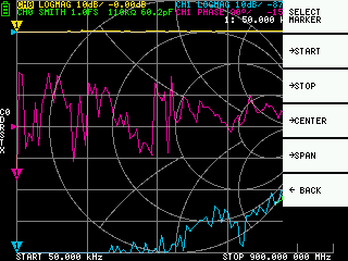
Setting the measurement frequency range
Recall calibration and settings
Setting sweep range and parameters
Appendix I – Hardware architecture
1 - Introduction
This user manual describes basic usage and operation of the NanoVNA V2 (S-A-A-2).
Note: OwOComm does not manufacture or market end user products including the NanoVNA V2.
For support please contact the seller you bought from.
Email address for engineering inquiries and project proposals:
OwOwOwOwO123@outlook.com (do not contact this address for customer support).
Please be aware: The earliest V2.2 design was open sourced and all clones are based on it. However, one vendor has been attempting to harm us by claiming credit for the design and deceiving customers, distributors, and the public that they originated the design. Please be aware and avoid the following products, which also exaggerate their specifications: LiteVNA, SAA-2N.
Credits
Copyright (C) 2021 OwOTech and cho45.
https://github.com/cho45/NanoVNA-manual
Relationship to the NanoVNA
The NanoVNA V2 hardware architecture is an entirely new, from-scratch design engineered to handle higher frequencies. However, the V2 firmware is a direct evolution of original developer edy555’s (ttrftech) core code, ported to C++11 and heavily optimized by the unified NanoRFE development team to support the new microwave-grade hardware. For details see Appendix I – Hardware architecture.
The USB interface is similar to the V1 in that it passes commands over a virtual serial port. However, much of the sweep and data transfer logic is reworked in order to support faster sweep rates and avoid data corruption. See Appendix II – USB data interface.
Specifications
Parameter |
Board version |
Specification |
Conditions |
Frequency range |
V2_2, V2 Plus |
50kHz - 3GHz |
- |
V2 Plus4, |
50kHz – 4.4GHz |
- |
|
Frequency resolution |
All |
0.01MHz |
- |
System dynamic range |
V2_2, V2 Plus |
60dB |
|
V2 Plus4 |
90dB |
AVG=20, 1GHz |
|
V2 Plus4 Pro |
90dB |
BW=1.6kHz, AVG=5, 1GHz |
|
96dB |
BW=1.6kHz, AVG=20, 1GHz |
||
S11 noise floor |
All |
-50dB |
f < 1.5GHz |
-40dB |
f < 3GHz |
||
Sweep points |
All |
1 – 1024 points (with NanoVNA-QT software). More points (up to 65535) are possible depending on the performance of your PC. Note: beware of clones that interpolate calibration to extend the number of sweep points on-device beyond 201 points, compromising accuracy, especially when using test cables. |
- |
Sweep time |
V2 Plus4 |
0.25s |
Default sweep settings |
V2 Plus4 Pro |
0.16s |
Default sweep settings |
|
Power supply |
All |
USB, 4.6V – 5.5V |
- |
Supply current |
All |
500mA typ |
No charging |
Battery current, charging |
All |
1.2A typ |
- |
Battery capacity |
V2 Plus4, |
3200mAh |
- |
Operation ambient temperature |
All |
0℃ - 45℃ * |
* by design, not tested in production |
Ambient temperature during battery charging |
All |
10℃ - 45℃ |
- |
VNA basics
A Vector Network Analyzer (VNA) measures the reflection and transmission behavior of a device under test (DUT) across a configured frequency range.
The NanoVNA V2 is a two port T/R (transmission/reflection) VNA which can measure the S parameters S11 and S21 of a two port network, or the reflection coefficient (S11) of a one port network.

Before any measurements are performed, the VNA must be calibrated. See section 3.1.Calibration for details.
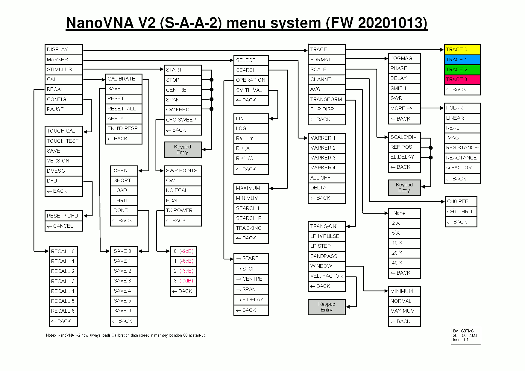
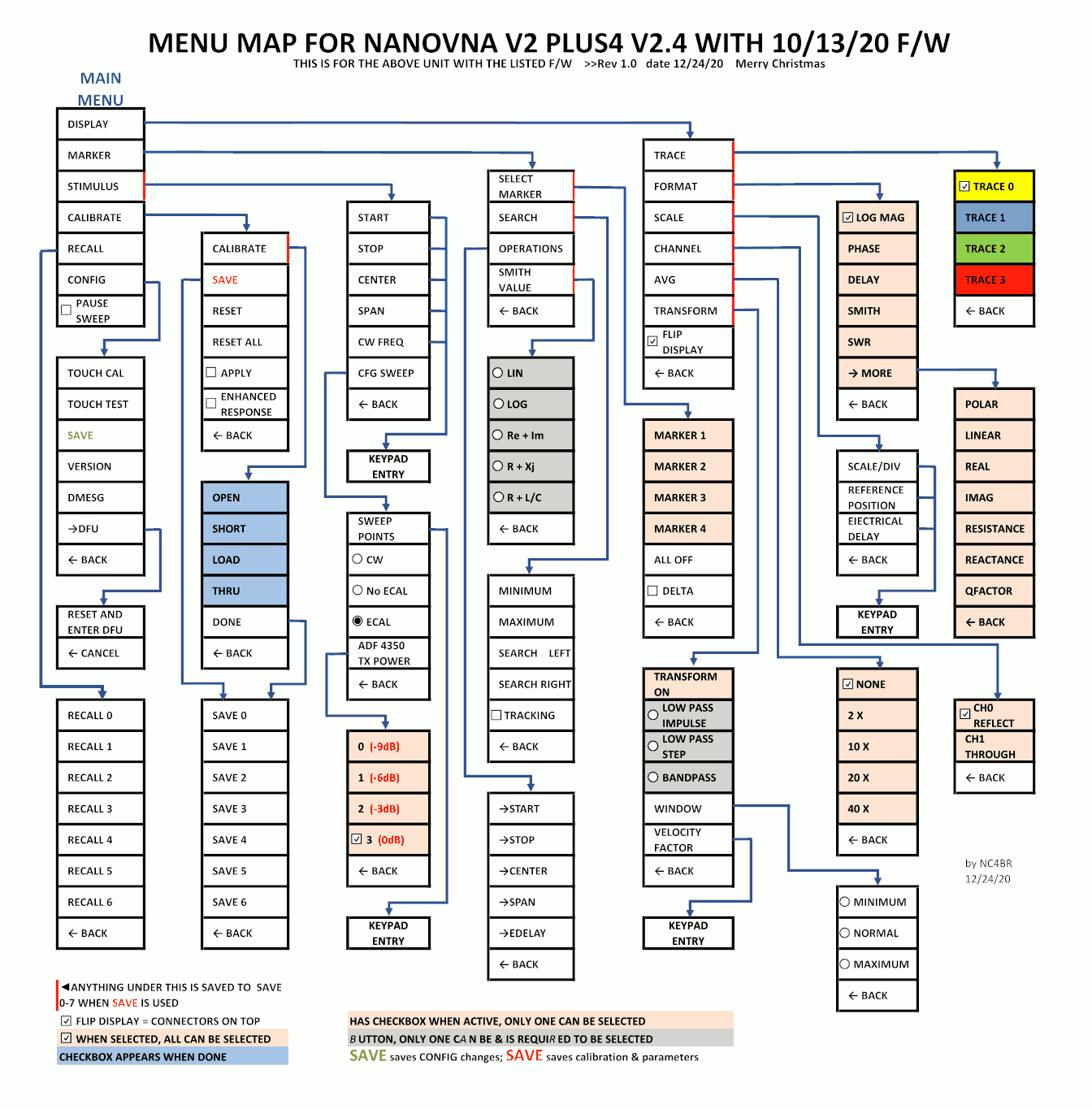
Menu map
2 - User interface
Main screen
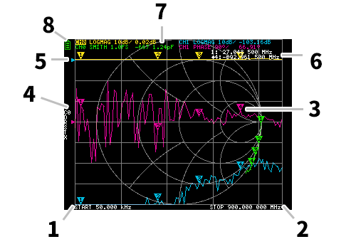
1. START frequency 2. STOP frequency
The START frequency and STOP frequency are shown at the bottom of the display.
3. Marker
The marker position for each trace is displayed as a small numbered triangle. The selected marker can be moved to any of the measured points in the following ways:
Drag a marker on the touch panel – best to use a stylus for this.
Press and hold the JOG LEFT or JOG RIGHT buttons.
4. Calibration status
Displays the saved slot number of the calibration being used and the error correction applied.
C0 C1 C2 C3 C4 : Each indicates that the corresponding calibration data is loaded.
D : Indicates that port 1 3-term error model is applied.
5. Reference position
Indicates the reference position of the corresponding trace. You can change the position with:
DISPLAY →SCALE →REFERENCE POSITION.
6. Marker status
The active marker that is selected and one marker that was previously active are displayed top right.
7. Trace status
The status of each trace format and the value corresponding to the active marker are displayed.
For example, if the display is showing: CH0 LOGMAG 10dB/ 0.02dB , read it as follows:
Channel CH0 (reflection)
Format LOGMAG
Scale is 10dB
Current value is 0.02dB
For active traces, the channel name is highlighted.
8. Battery status
This is not shown on the NanoVNA V2. Battery percentage is indicated by the 4 red LEDs along the left side on the bottom of the device.
Menu screen
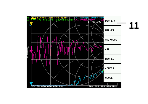
11. Menu List
The menu can be opened by the following operations:
When a location other than a marker on the touch screen is tapped.
When the ENTER button is pressed.
Keypad screen
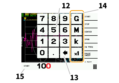
12. Numeric keys
Tap a number to enter one character.
13. Back key
Delete one character. If no character is entered, the entry is canceled and the previous state is restored.
14. Unit key
Multiplies the current input by the appropriate unit and terminates input immediately. In case of × 1, the entered value is set as it is.
15. Input field
The name of the item to be entered and the entered number are displayed.
Device settings
The CONFIG menu contains general settings for the device:
Saving device settings
Select CONFIG →SAVE to save general instrument settings. General device settings are data that includes the following information:
Touch screen calibration information
Grid color
Trace color
The CONFIG →SAVE command does not apply to calibration settings.
Display version info
Select CONFIG →VERSION to display device version information.
Firmware update mode
CONFIG →BOOTLOAD. Select RESET AND ENTER to reset the device and enter BOOTLOAD mode. In this mode, firmware can be updated via USB.
BOOTLOAD mode can also be entered by holding down the “left” push button while the device is powered off and on.
See section 5.5.Firmware Update for how to update the device firmware using the NanoVNA-QT PC software.
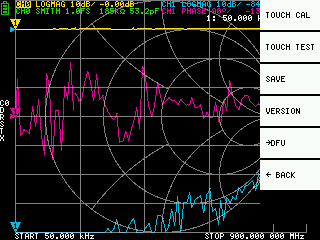
Touch panel calibration and testing
The LCD touch panel can be calibrated using CONFIG → TOUCH CAL if there is a large difference between the actual on-screen tap position and the recognized tap position.
NOTE: Be sure to save the settings with CONFIG → SAVE.


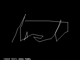
You can then test the LCD touch panel stylus tracking accuracy by selecting CONFIG → TOUCH TEST.
A line is drawn while dragging the stylus along the touch panel. When released from the touch panel, it returns to its original state. Repeat & save the touch screen calibration if tracking is incorrect.
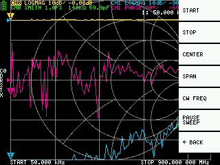
3 - Performing measurements
The basic measurement sequence is:
Set the frequency range to be measured.
Use STIMILUS → START/STOP or STIMILUS → SPAN/CENTERPerform calibration (and save!)
Connect the Device Under Test (DUT) and measure.
Setting the measurement frequency range
There are three types of measurement range settings.
Setting the start frequency and stop frequency
Setting the center frequency and span
Zero span
Setting the start frequency and stop frequency
Select and set STIMULUS → START and STIMULUS → STOP, respectively.
Setting the center frequency and span
Select and set STIMULUS → CENTER and STIMULUS → SPAN, respectively.
Zero span
Zero span is a mode in which one frequency is sent continuously without frequency sweep.
Select and set STIMULUS → CW FREQ.
Temporarily stop measurement
When menu item PAUSE SWEEP is active, measurement is temporarily stopped.
Calibration
Calibration must be performed whenever the frequency range to be measured is changed. When calibration is activated, the left side of the screen should show “Cx” and “D”.
Changing the frequency sweep range always clears the active calibration, if any.
The calibration procedure is as follows:
Reset current calibration state. Select menu item CAL →RESET and then →CALIBRATE.
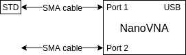
Attach a SMA coaxial cable to port 1.
(Optional) Attach a SMA coaxial cable to port 2.
Connect OPEN standard to port 1 cable and click →OPEN. Wait for menu item highlight.
Connect SHORT standard to port 1 cable and click →SHORT. Wait for menu item highlight.
Connect LOAD standard to port 1 cable and click →LOAD. Wait for menu item highlight.
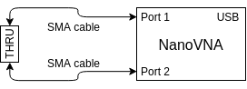
(Optional) Connect the THRU standard between the port 1 and port 2 cable ends, and click →THRU.
Click →DONE.
Specify the dataset number (0 to 4) and save. e.g. →SAVE 0.
 Measuring
a calibration standard
Measuring
a calibration standard
 Measuring
the THRU standard
Measuring
the THRU standard
Note that there is no need to wait for the plots to fully update after connecting a calibration standard. Clicking any of the OPEN, SHORT, LOAD, THRU calibration menu items will perform a full sweep with 2x averaging. Once the sweep is complete the corresponding menu item will become highlighted, and you may proceed to the next calibration standard.
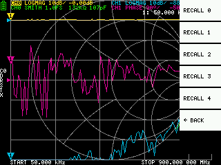
Trace display
Up to four traces can be displayed, one of which is the active trace.
You can turn on/off traces as needed. The menu items DISPLAY →TRACE →TRACE n allow you to activate as well as turn on/off traces.
When a trace is active, its channel name at the top of the screen is highlighted. In the image above, TRACE 0 is the active trace.
Clicking DISPLAY →TRACE →TRACE n on the current active trace will turn it off. Clicking any other trace activates it.
Trace format
Although each trace can have its own displayed format, you can only change the format of the active trace.
To assign a format, set the trace to active (see above) then select: DISPLAY →FORMAT
The description and unit of measurement of each format is as follows:
LOGMAG : Logarithm of absolute value of measured value (dB per div)
PHASE : Phase in the range of -180 ° to + 180 ° (90 degree default)
DELAY : Delay (pico or nano seconds)
SMITH : Smith Chart (Impedance scale is normalized during calibration)
SWR : Standing Wave Ratio (can be scaled to show 1, 0.1 or 0.01 per div)
POLAR : Polar coordinate format (Impedance scale is normalized during calibration)
LINEAR : Absolute value of the measured value
REAL : Real part of measured S parameter
IMAG : Imaginary part of measured S parameter
RESISTANCE : Resistance component of the measured impedance (ohms per div)
REACTANCE : Reactance component of the measured impedance (ohms per div)
Trace channel
The NanoVNA V2 has two channels, CH0 and CH1, corresponding to ports 1 and 2.
CH0 is the S parameter S11, while CH1 is the S parameter S21.
Each trace can be set to display data from either channel.
To change the channel used by the currently active trace, select
DISPLAY →CHANNEL →CH0 REFLECT or DISPLAY →CHANNEL →CH1 THROUGH.
Markers
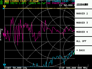
Up to 4 markers can be displayed.
Markers are selected by the menu items MARKER →SELECT MARKER →MARKER n .
Clicking on a disabled marker menu item enables it and makes it active. Clicking on an enabled but non-active marker activates it. Clicking on the currently active marker disables it.
Setting frequencies from marker(s)
You can set the frequency range from the MARKER →OPERATIONS menu as follows:
OPERATIONS →START - Sets the start frequency to the active marker’s frequency.
OPERATIONS →STOP - Sets the stop frequency to the active marker’s frequency.
OPERATIONS →CENTER - Sets the frequency of the active marker to be the center frequency.
OPERATIONS →SPAN - Sets the absolute frequency span to the last two active markers. You need to have any two markers (M1-M4) enabled for the Span button to work. If only one marker is displayed, nothing happens.
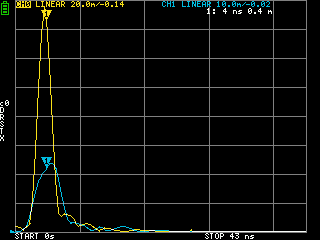
Time domain operation
The NanoVNA V2 can simulate time domain reflectometry by transforming frequency domain data.
Select DISPLAY →TRANSFORM →TRANSFORM ON to convert measured data to the time domain.
If TRANSFORM ON is enabled (Inverted white text on black background), the measurement data is immediately converted to the time domain and displayed. The relationship between the time domain and the frequency domain is as follows.
Increasing the maximum frequency increases the time resolution
The shorter the measurement frequency interval (ie, the lower the maximum frequency), the longer the maximum time length
For this reason, the maximum time length and time resolution are in a trade-off relationship. In other words, the time length is the distance.
If you want to increase the maximum measurement distance, you need to lower the frequency spacing (frequency span / sweep points).
If you want to measure the distance accurately, you need to increase the frequency span.
HINT – Use a lower frequency to measure a longer length and a higher frequency to measure a shorter length and adjust accordingly for accurate results.
Time domain bandpass
In bandpass mode, you can simulate the DUT response to an impulse signal.
NOTE: The trace format can be set to LINEAR, LOGMAG or SWR.
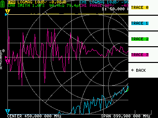
The following is an example of the impulse response of a bandpass filter.
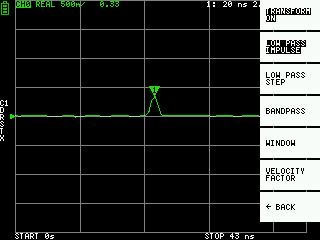
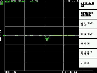
Time domain low pass impulse
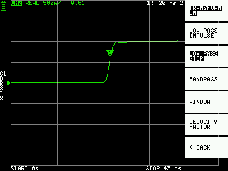
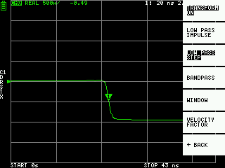
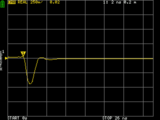
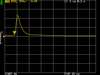
In low-pass mode, you can simulate TDR. In low-pass mode, the start frequency must be set to 50 kHz, and the stop frequency must be set according to the distance to be measured.
The trace format can be set to REAL.
Examples of Impulse response in open state and impulse response in short state are shown below.
Open |
Short |
|
|
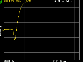
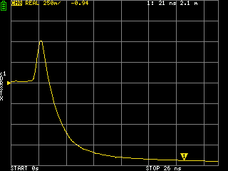
Time domain low pass step
The trace format can be set to REAL.
Example measurements of Step response are shown below.
Open |
Short |
|
|
Capacitive short |
Inductive short |
|
|
Capacitive discontinuity (C in parallel) |
Inductive discontinuity (L in series) |
|
|
Time domain window
The range that can be measured is a finite number, and there is a minimum frequency and a maximum frequency. A window can be used to smooth out this discontinuous measurement data and reduce ringing.
There are three levels of windowing.
MINIMUM (no window, ie: same as rectangular window)
NORMAL (equivalent to Kaiser window β = 6)
MAXIMUM (equivalent to Kaiser window β = 13)
MINIMUM provides the highest resolution and MAXIMUM provides the highest dynamic range. NORMAL is in the middle.
Setting the velocity factor in the time domain
The transmission speed of electromagnetic waves in the cable varies depending on the material. The ratio to the transmission speed of electromagnetic waves in vacuum is called the Velocity Factor. This is always stated in the cable specifications.
In the time domain, the displayed time can be converted into distance. The wavelength shortening ratio used for distance display can be set with DISPLAY → TRANSFORM → VELOCITY FACTOR .
For example, if you measure the TDR of a cable with a wavelength reduction rate of 67%, specify 67 for the VELOCITY FACTOR. (Do not use the decimal point).
Recall calibration and settings
Up to 5 calibration datasets can be saved.
Calibration data includes the following information:
Frequency range setting
Error correction at each measurement point
Trace settings
Marker settings
Domain mode settings
Electrical delay
You can save the current settings by selecting CAL → SAVE → SAVE n.
Current calibration data can be reset by selecting CAL → RESET.
CAL → CORRECTION indicates whether error correction is currently enabled. You can deselect this to temporarily disable error correction. (Inverted text=ON, Normal text=OFF)
RECALL the saved settings by selecting CAL → RECALL → RECALL n.
4 - NanoVNA-QT Software
This chapter describes the usage of the NanoVNA-QT PC software with the NanoVNA V2.
NanoVNA-QT is derived from software for the xaVNA.
Platforms supported: Linux, Windows (7+), Mac OS (10.11+)
User interface
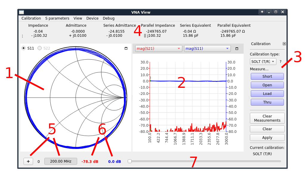
1 – Smith chart display
Shows a smith chart of S11 or S22 depending on the radiobutton selected.
2 – Line graph display
Shows a line graph plot of two user selected traces. The two dropdown lists above the graph select the data source displayed. The color of the trace corresponds to the color of the dropdown.
3 – Calibration pane
Allows you to measure calibration standards and enable/disable calibration.
4 – Impedance display
Shows impedance values and series/parallel equivalent circuits calculated from S11.
5 – Marker control 6 – Marker values
The “+” button adds a new marker. Clicking on the frequency indicator will show/hide the marker dot. Labels show the numeric value of each line graph trace at the current marker frequency.
7 – Marker slider
Adjust this slider to control marker position.
Connecting to the device
After connecting the device to the PC using a USB cable, a new serial port device should show under the Device menu in NanoVNA-QT. If no device shows up, you may need to install the Cypress USB Serial driver (can be found on NanoVNA-QT binary release downloads). The device uses the USB CDC class, which does not require dedicated drivers on Linux and Mac OS.
Select the device under the Device menu to connect to it. Continuous sweep will start immediately and you should see continuously updating data on the smith chart and line plots.
Setting sweep range and parameters
Click Device > Sweep parameters… from the main menu to bring up the Sweep Parameters dialog.
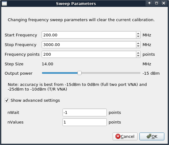
Settings:
Start frequency/Stop Frequency control the sweep frequency range.
Frequency points is the number of discrete frequency points.
Output power is not applicable to the NanoVNA V2 and the setting is ignored.
Under Show advanced settings:
nWait is not applicable to the NanoVNA V2 and the setting is ignored.
nValues controls the number of data points per sweep point to average over. Setting a higher averaging factor will result in proportionally lower noise and higher sweep times.
Calibration
Calibration in the NanoVNA-QT UI is similar to the on-device UI.
Calibration must be performed whenever the frequency range to be measured is changed. When calibration is activated, the label under “Current calibration” in 3 – Calibration pane will indicate the current calibration type. “None” indicates no calibration is active.
Changing the frequency sweep range always clears the active calibration, if any.
The calibration procedure is as follows:
Reset current calibration. Click Clear and Clear Measurements under 3 – Calibration pane.
Select Calibration type. Use SOL (1 port) to correct for S11 only, and use SOLT (T/R) to correct for S11 and S21 response. Other calibration types in the dropdown list apply to full two port VNAs only and are not applicable to the NanoVNA V2 which is a T/R VNA.
Attach a SMA coaxial cable to port 1.
(SOLT only) Attach a SMA coaxial cable to port 2.
Connect OPEN standard to port 1 cable and click Open. Wait for button highlight.
Connect SHORT standard to port 1 cable and click Short. Wait for button highlight.
Connect LOAD standard to port 1 cable and click Load. Wait for button highlight.
(SOLT only) Connect the THRU standard between the port 1 and port 2 cable ends, and click Thru. Wait for button highlight.
Click Apply.
Refer to the figures in section 3.1.Calibration for how to connect the calibration standards.
Note that there is no need to wait for the plots to fully update after connecting a calibration standard. Clicking any of the Open, Short, Load, Thru buttons will perform a full sweep with 2x averaging. Once the sweep is complete the button will become highlighted, and you may proceed to the next calibration standard.
To save the current calibration click Calibration > Save as… in the main menu.
To recall a saved calibration click Calibration > Load… in the main menu. Recently saved or recalled calibrations will also be listed under the Calibration menu and can be selected directly.
Saved calibration files contain the measurements for each calibration standard. Recalling a saved calibration file will calculate a new calibration using the old (saved) measurements and the currently configured calibration kit parameters.
Calibration kit parameters
NanoVNA-QT supports user calibration kit parameters. Click Calibration > Kit settings under main menu to open the Calibration kit parameters dialog.
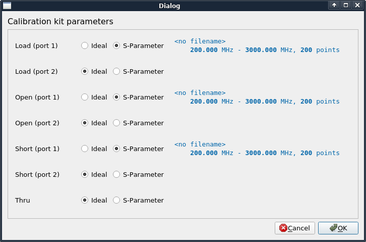
Each calibration kit type can be associated with an S parameter model, or an ideal model can be used. Clicking on the S-Parameter radio button will bring up a file chooser dialog to select the S parameter file.
Note: these kit parameters are global and are not associated with a calibration save file. If you modify kit parameters and proceed to recall an older calibration file, the old calibration will be re-calculated using the newly configured kit parameters!
Firmware Update
The NanoVNA-QT software has built in support for updating the firmware on the NanoVNA V2.
To perform a firmware update:
Connect the device to a PC using a USB cable.
Put the device into BOOTLOAD mode. This can be done from the device menu by selecting CONFIG →BOOTLOAD, and selecting RESET AND ENTER. BOOTLOAD mode can also be entered by holding down the JOG LEFT button on the device while it is powered off and on.
The device should appear under the Device menu in NanoVNA-QT.
Click the device under the Device menu, for example /dev/ttyACM0.
You will be prompted to update the device firmware. Answer “yes” or “update firmware”.
You will be prompted to select a firmware raw binary file. Select the file you wish to flash.
Firmware update will begin and progress is shown in NanoVNA-QT.
If the firmware update fails or is interrupted, go to step 2 and retry.
After the firmware update is complete, the device will automatically reboot into the new firmware. You can now connect to the device in NanoVNA-QT.
5 - Appendix I – Hardware architecture
The NanoVNA V2 is a highly cost optimized design that aims to achieve the best possible RF performance within a tight BOM budget.
The following block diagram shows a high level overview of the system.
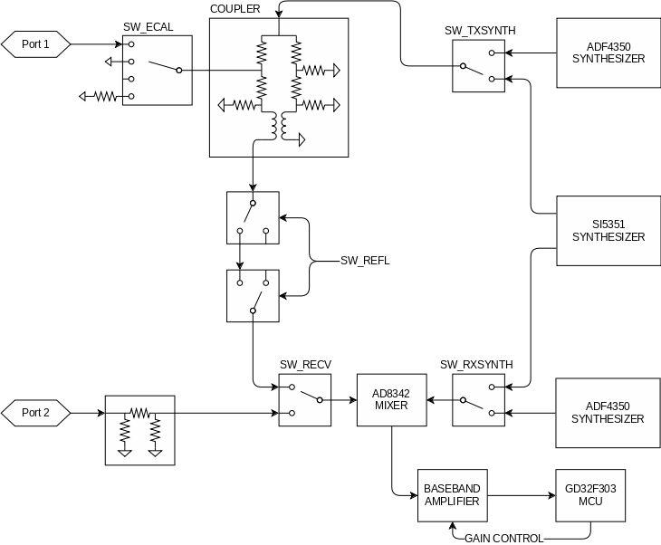
The NanoVNA V2 is a single switched receiver VNA. While the diagram shows only two channels selectable by the receive mixer through SW_RECV, a third channel, the reference channel, is provided by setting SW_ECAL to the “open circuit” position. By controlling these two switches the receiver is able to observe reference, reflected, and thru signals.
Signal generators
Two ADF4350 RF synthesizers, plus one Si5351, provide the stimulus and LO signals. The Si5351 covers frequencies up to 140MHz, and the rest are covered by the ADF4350s.
Directional coupler
The coupler is based on a Wheatstone bridge rearranged so that input and DUT ports are referenced to ground. The coupled signal exists as a difference signal and is extracted by baluns. Two stages of baluns are used to achieve the necessary common mode rejection ratio.
Receiver
The receiver consists of a AD8342 mixer and an op-amp based baseband amplifier.
The mixer downconverts the RF signal to a low but nonzero intermediate frequency (typically 12kHz). The IF signal is digitized using the built in 12 bit ADCs on the GD32 microcontroller.
Firmware on the microcontroller digitially detects the phase and magnitude of the IF, and thus RF signal, which results in superior accuracy compared to VNAs using a phase and magnitude detector IC that does the detection in the analog domain.
6 - Appendix II – USB data interface
The NanoVNA V2 appears as a USB CDC (Communications Device Class) virtual serial port both during normal operation and in BOOTLOAD mode. PC software can issue commands and request data by sending and receiving data on the virtual serial port. Communications protocol is identical in the two cases, with only register layouts differing.
Protocol description
Only the host may initiate commands by sending one or more bytes on the virtual serial port. Each command may have a different length. There is no separator delimiting each command.
The device may not send data to the host except for replies to a host-to-device command.
The following table lists all supported commands and their byte encodings, and is applicable both during normal operation and in BOOTLOAD mode.
Host to device command list
All byte values in the table are in hexadecimal. B0 to B5 denote bytes 0 to 5. B0 is the opcode.
B0 |
B1 |
B2 |
B3 |
B4 |
B5 |
Name |
Description |
00 |
- |
- |
- |
- |
- |
NOP |
No operation |
0d |
- |
- |
- |
- |
- |
INDICATE |
Device always replies with ascii ‘2’ (0x32) |
10 |
(AA) |
- |
- |
- |
- |
READ |
Read a 1-byte register at address AA. Reply is one byte, the read value. |
11 |
(AA) |
- |
- |
- |
- |
READ2 |
Read a 2-byte register at address AA. Reply is 2 bytes, the read value. |
12 |
(AA) |
- |
- |
- |
- |
READ4 |
Read a 4-byte register at address AA. Reply is 4 bytes, the read value. |
18 |
(AA) |
(NN) |
- |
- |
- |
READFIFO |
Read NN values from a FIFO at address AA. Reply is the read values in order. Each value can be more than one byte and is determined by the FIFO being read. |
20 |
(AA) |
(XX) |
- |
- |
- |
WRITE |
Write XX to a 1-byte register at address AA. There is no reply. |
21 |
(AA) |
(X0) |
(X1) |
- |
- |
WRITE2 |
Write X0 to AA, then X1 to AA+1. There is no reply. |
22 |
(AA) |
(X0) |
(X1) |
(X2) |
(X3) |
WRITE4 |
Write X0..X3 to registers starting at AA. There is no reply. |
23 |
(AA) |
(X0) |
(X1) |
(X2) |
... |
WRITE8 |
This command is 10 bytes in total. Bytes 2..9 correspond to X0..X7. Write X0..X7 to registers starting at AA. There is no reply. |
28 |
(AA) |
(NN) |
… |
|
|
WRITEFIFO |
Write NN bytes into a FIFO at address AA. NN bytes of data to be written into the FIFO should follow “NN”. There is no reply. |
Register descriptions
The following table lists all registers accessible during normal operation.
All addresses are in hexadecimal.
Multi-byte integer registers are encoded in Little Endian. Lowest numbered registers contain the least significant portions of the integer.
Address |
Name |
Description |
00..07 |
sweepStartHz |
Sets the sweep start frequency in Hz. uint64. |
10..17 |
sweepStepHz |
Sets the sweep step frequency in Hz. uint64. |
20..21 |
sweepPoints |
Sets the number of sweep frequency points. uint16. |
22..23 |
valuesPerFrequency |
Sets the number of data points to output for each frequency. uint16. |
26 |
rawSamplesMode |
Writing 1 switches USB data format to raw samples mode and leaves this protocol. |
30 |
valuesFIFO |
Returns VNA sweep data points. Each value is 32 bytes. Writing any value (using WRITE command) clears the FIFO. See FIFO data format section below. |
f0 |
deviceVariant |
The type of device this is. Always 0x02 for NanoVNA V2. |
f1 |
protocolVersion |
Version of this wire protocol. Always 0x01. |
f2 |
hardwareRevision |
Hardware revision. |
f3 |
firmwareMajor |
Firmware major version. |
f4 |
firmwareMinor |
Firmware minor version. |
Remarks
sweepStartHz, sweepStepHz, and sweepPoints together set the sweep parameters of the VNA.
Writing any value to these registers will immediately terminate the on-device UI and put the device in “USB data mode”, where the PC has full control over VNA operation.
You can not observe user entered sweep parameters (from the device UI) by reading these registers.
Sweep is always running and can not be paused.
FIFO data format
The values read from valuesFIFO are 32 bytes each. The following table lists the fields in each value. All byte offsets are in hexadecimal. All multi-byte integers are encoded in Little Endian. Lowest numbered bytes contain the least significant portions of the integer.
Bytes |
Name |
Description |
Type |
00..03 |
fwd0Re |
Real part of channel 0 outgoing wave. |
int32 |
04..07 |
fwd0Im |
Imaginary part of channel 0 outgoing wave. |
int32 |
08..0b |
rev0Re |
Real part of channel 0 incoming wave. |
int32 |
0c..0f |
rev0Im |
Imaginary part of channel 0 incoming wave. |
int32 |
10..13 |
rev1Re |
Real part of channel 1 incoming wave. |
int32 |
14..17 |
rev1Im |
Imaginary part of channel 1 incoming wave. |
int32 |
18..19 |
freqIndex |
Frequency index, 0 to sweepPoints - 1. |
uint16 |
1a..1f |
(reserved) |
(reserved) |
- |
valuesFIFO is continuously being filled with new sweep data regardless of whether it is being read. If you wish to do on-demand sweeps, it is necessary to clear stale data before reading from the FIFO. The FIFO can be cleared by writing (with the WRITE command) any value to the FIFO address.
valuesFIFO returns raw values representing the in-phase and quadrature part of the measured waves, which never have user calibration applied. You can not access the on-device user calibrations or calibrated data over USB.
fwd0Re/fwd0Im is referred to as the reference channel. All complex values read from valuesFIFO can be at a random phase, so you must divide (using complex division) each value by the reference channel to get absolute phase and magnitude values.
Register descriptions (BOOTLOAD mode)
The following table lists all registers accessible in BOOTLOAD mode.
All addresses are in hexadecimal.
Multi-byte integer registers are encoded in Little Endian. Lowest numbered registers contain the least significant portions of the integer.
Address |
Name |
Description |
e0..e3 |
flashWriteStart |
Current flash write address. uint32. Set this to the address to start writing at. |
e4 |
flashFIFO |
Writing to this FIFO will write data into flash starting at flashWriteStart. flashWriteStart will be incremented by the number of bytes written. |
e8..eb |
userArgument |
The user argument to pass to the program upon soft reset. uint32. |
ef |
doReboot |
Write 0x5e to initiate a soft reset. |
f0 |
deviceVariant |
The type of device this is. Always 0x02 for NanoVNA V2. |
f1 |
protocolVersion |
Version of this wire protocol. Always 0x01. |
f2 |
hardwareRevision |
Hardware revision. Always 0x00 in BOOTLOAD mode. |
f3 |
firmwareMajor |
Firmware major version. Always 0xff in BOOTLOAD mode. |
f4 |
firmwareMinor |
Firmware minor version (of the bootloader). |
Writing to flash
The procedure to write a new firmware image to flash are as follows.
Connect the device to the PC over USB and put the device into BOOTLOAD mode.
Open the virtual serial port in raw mode (platform specific).
Write the address you wish to start flashing from to flashWriteStart.
Use the WRITEFIFO command to send up to 255 bytes at a time to flashFIFO.
Each WRITEFIFO command can be followed with a INDICATE command, which will reply with ‘2’ only after the flash operation is complete.
There is no flow control on the virtual serial port and you must limit the amount of outstanding writes to no more than 2048 bytes.(Optional) Write 0x5e to doReboot to soft reset the device.