Beware of cheap underperforming clones

As of 2022 there are many badly performing clones on the market. V2/3GHz NanoVNA uses parts like ADF4350 and AD8342 which are costly and clones have been cutting costs by using salvaged or reject parts.

See official store and look for V2 Plus4/V2 Plus4 Pro versions only to avoid getting a bad clone. We have stopped selling V2.2 versions since October 2020, so all V2 hardware that are not Plus or Plus4 are not made by us and we can not guarantee performance.

NanoVNA V2 Forum

Note: this page is a mirror of https://groups.io/g/NanoVNAV2.
Click here to join and see most recent posts.

new firmware


iz1fks 2020/09/26 03:48

hello,

I have instaled latest firmware *20200926 for V2.2* but the manu on the left cannot be used since after clicking any key the menu disappear. I had to downgrade to previus version

Phil *
*

Siegfried Jackstien 2020/09/26 12:49

Phil

use the push buttons to select touch screen calibration

calibrate your touch and STORE the calibration

greetz sigi dg9bfc


Am 26.09.2020 um 10:48 schrieb iz1fks:

mce66 2020/09/26 12:51

Hello,

I installed FW 20200926 (for 3.2 inch LCD) and I think I found a bug (maybe also spotted a few days ago in an interim FW version by Kurt). The CH1 LOGMAG (S21) seems to jump 0/-1db randomically. I attach 4 pictures:

* Picture 1 is a 3 dB splitter. S21 seems perfectly reported by NanoVNA
* Picture 2 is the same splitter, but the calibration was obtained adding a 10 dB attenuator in front of Nano RX port. You can see that the S21 is OK only in some parts of the spectrum and is -1dB in some other. (Note anyway the improvement of S11 reading ...)
* Picture 3 is a 10 dB attenuator: S21 seems perfect.
* Picture 4 is a 20 dB attenuator: again in some parts of the spectrum the S21 is -1dB with respect to the right value.

For your troubleshooting: the issue is independent from Enhanced Response Flag, Some difference occurs instead selecting different Averaging (the -1dB occurs at different frequencies, but still it is exactly -1 dB).

Available for any additional test.

Best Regards, Marco.

Siegfried Jackstien 2020/09/26 20:19

no wonder if you have a dut (your 3 db splitter) with input match of 20
db(look in mid  of your range)  ... and you measure over a 10 db
attenuator added to s11 port you see a 40 db return loss (cause
reflected energy travels TWO times trough your 10 db attenuator)

greetz sigi dg9bfc

ps .. hmmm i thought we had that 1 db fault solved ?!?!?!?! HMMM?!?!?

Am 26.09.2020 um 19:51 schrieb mce66:

mce66 2020/09/26 13:51

Hello Siegfried. The attenuator in second measurement is not on splitter input but on splitter output (the other is loaded). The problem is that the Return Loss of my NanoVNA RX port is quite bad (peaks 13 dB at 2.5 GHz). This means that the output port of the splitter is not perfectly loaded. The input of the spitter "feels" the mismatch of the output port and the measure of S11 is worse than real splitter performance. If I put the 10 dB attenuator at the output of the splitter and before the input of the VNA, I'm improving the RL of the VNA input and then the splitter is much better loaded on output and then its S11 results much closer to the spec. Please note also that all dB scales are 5 dB/Div.

Finally, if I just put two "very good" loads at the two outputs of the splitter, I obtain a perfect S11 measurement (25 dB return loss at center band, no added ripple). This Slitter (Jfw 50PD-659) is rated 698-3000 MHz. Of course I lose in this wat the possibility to contemporary measure S21... Picture of S11 with 2 loads attached.

Best Reagards, Marco.

Siegfried Jackstien 2020/09/27 02:02

why is return loss low on your rx port??? should be better ...

dg9bfc sigi

Am 26.09.2020 um 20:51 schrieb mce66:

OwO 2020/09/27 14:36

@mce66: See if the attached firmware (for V2_2 2.8/3.2 inch) affects the
1dB jump, and if possible can you tell me the DEBUG1 and DEBUG2 values
in CONFIG > DMESG with this firmware?

On 27/09/2020 03:51, mce66 wrote:

mce66 2020/09/27 02:28

Hello OwO, with your debug FW the issue looks the same as before. I must say I zoomed in better and the jump is not exactly 1 dB but seems about 0.7 dB. Attached a picture with CH1 LOGMAG at 1 dB/Div. Attached also the DMESG with your debug FW.

Fell free to ask for any additional test.

Best regards, Marco.

OwO 2020/09/27 18:13

Ok, try this firmware, I made some small tweaks on the AGC logic:

iz1fks 2020/09/27 08:36

thanks, It was the first time with this issue after firmware upgrade.

regards

Phil

mce66 2020/09/27 08:58

Hello OwO, It seems that with this second debug version the issue is solved. I've limited testing capability but the cases I've seen before (as reported in my post) are now solved. I attach the DMESG of this second debug FW since numbers are a bit different (just for your double check).

Best Regards, Marco.

OwO 2020/09/28 00:55

Ok, I think I know what the cause of the issue is now. Unfortunately the
fix depends on characteristics of the signal path, and there seems to be
large differences between hardware variants (probably because of parts
substitutions) so I'm going to need to release separate binaries for
each variant in the next release.

On 27/09/2020 23:58, mce66 wrote:

mce66 2020/09/27 10:03

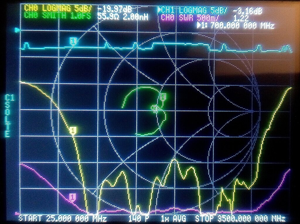
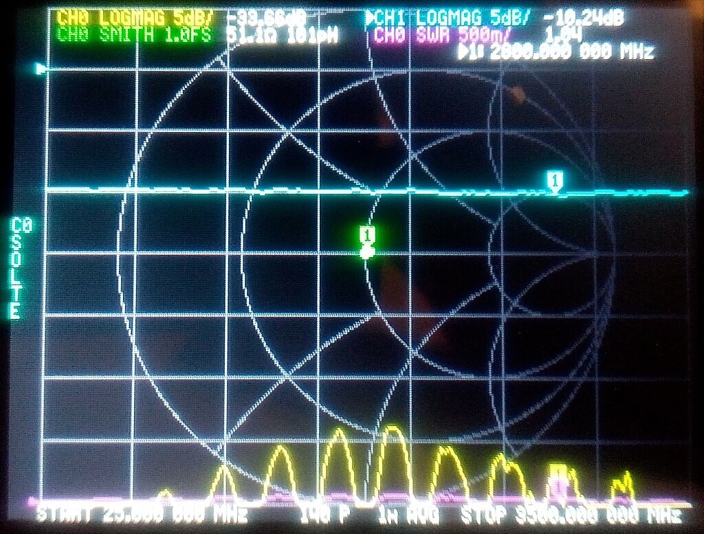
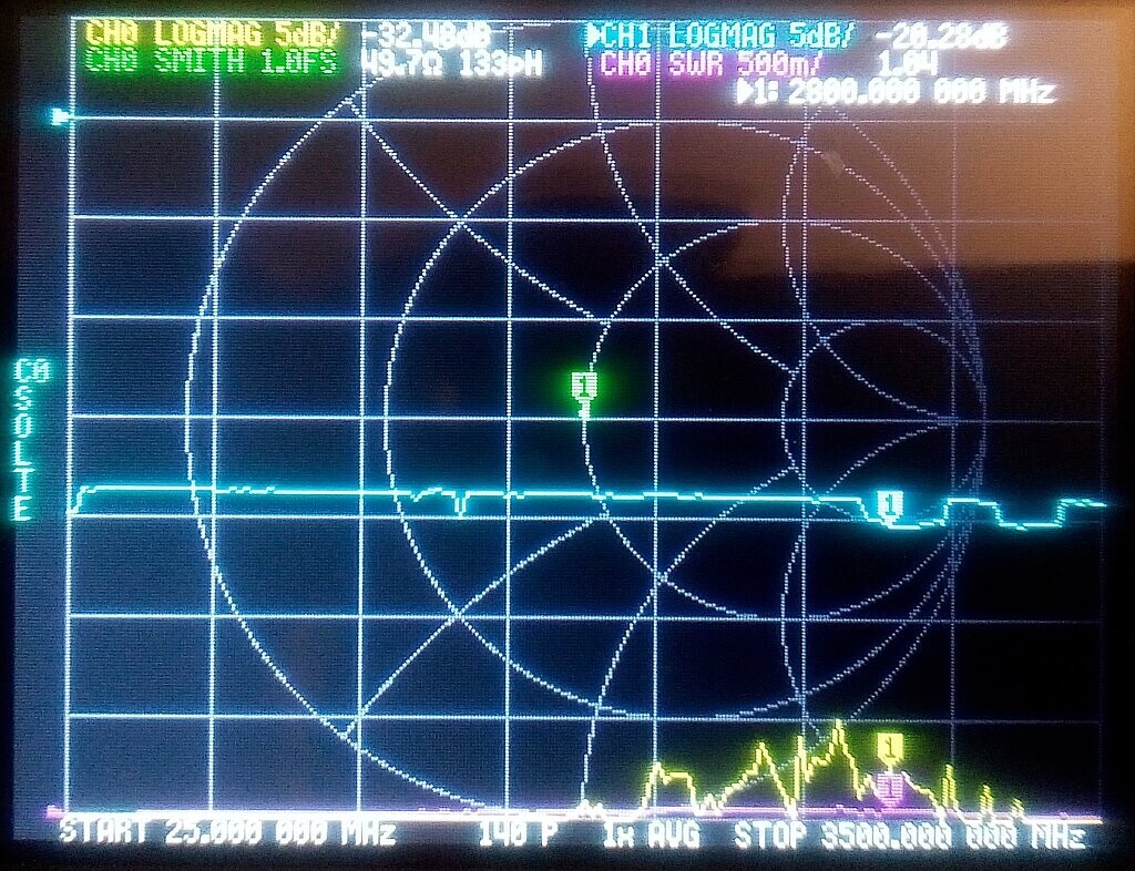
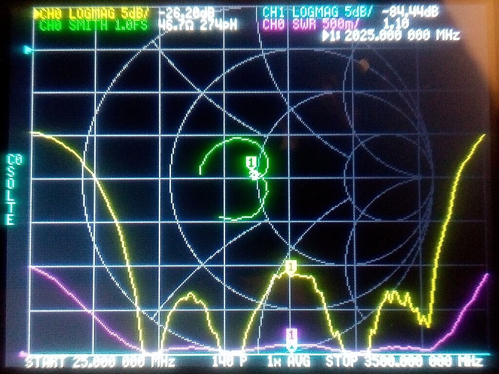
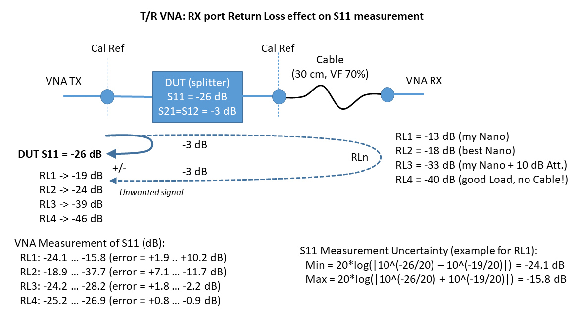
Hello Siegfried, to clarify the S11 measurement uncertainty, I just prepared the figure attached to this post.

My Nano is not perfect but even with a better Nano or any other T/R VNA (e.g. RL 18 dB) the situation would not change so much, We are facing here the limitation of the T/R VNA that cannot correct for the RX port mismatch during measurements of both S11 and S21. I made 4 examples with 4 different VNA input RL: 13 dB (my Nano), 18 dB (best Nano), 33 dB (my Nano plus 10 dB attenuator between DUT Out and the Cable), 40 dB (a good Load, directly connected to DUT Out without any cable). You can see that the signal to be measured (S11) will be disturbed by the unwanted signal passing through the DUT, reflected by VNA input mismatch and passing back the DUT. This unwanted signal sums/subtracts (depending on frequency and Cable/DUT/VNA delay) to the S11 reflected by DUT and then the S11 measurement by VNA presents a ripple that can be form many dB (the unwanted signal can be higher than the DUT S11...) to few tents of dB (Load case).

The case of a DUT with low attenuation in both directions and with a low S11 Return Loss to be measured is the worst case for T/R VNA. The only solution is to put a good 10 dB attenuator (i.e. with low RL) between DUT Out and the Cable (of course, VNA thru calibration shall be done with this attenuator already inserted between TX and RX VNA cables). Best S11 measurement can be obtained by terminating the DUT output with a good load, so totally disconnecting the VNA RX port.

At last, S11 measurement uncertainties with this "difficult" DUT are:

* +10...+2 dB (my Nano)
* +7...-12 dB (best Nano)
* +2...-2 dB (my Nano + 10 dB Att)
* +1...-1 dB (a good Load)

Best Regards, Marco.

mce66 2020/09/27 10:38

Hello OwO,

What you say is not good since you are hard coding in the FW some HW "analog" characteristics/calibrations. I think that the characteristics of the signal pah depends not only on the different HW versions, but also on temperature. I attach the new DMESG of a reboot after a hour warm-up: you can see that numbers (expecially DEBUG1 and 2 numbers) are changing again. Hope the solution will handle these drifts.

It is not good also because you need to relase many SW versions and you need to know in advance the signal path characteristics of all different HW versions... Instead, it is assumed that SOLT is the only "analog" calibration needed to characterize the different HW.

Best Regards, Marco.

OwO 2020/09/28 01:52

I'll have a think about that and see what I can come up with.

On 28/09/2020 01:38, mce66 wrote:

mce66 2020/10/14 12:06

Hello,

I've seen the new FW 20201013 reporting in changelog "AGC bugfixes". Do you know if this new version solved the issue of the 1 dB random jumps in S21 for all kind of HardWare?

I've another question: the calibration of the four AGC gains is performed only at power-on or on a regular bases? I think that the temperature drift after power-on may cause some non-linearity errors in AGC if the internal gain calibration is not repeated from time to time (e.g. every minute or every 100 sweeps or so).

Thanks, Marco.

To reply to this topic, join https://groups.io/g/NanoVNAV2

View this thread on groups.io