Anish Mangal 2022/04/07 19:02
Hi,
Thanks for the responses. I understand the logic behind load pull measurements, and I do not have the equipment (two directional couplers capable of handling 100W) necessary to perform load pull measurements.
I am trying to design a class-A P.A. capable of ~100-20W RF Power out in the 88-108MHz band.
The transistor I'm using is the MRF300AN. Though I don't need it's max 300W drive power, it has a lower case to junction thermal resistance than its lower power sibling - MRF101AN. I also needed a driver stage (because the source of the signal is a low power LimeSDR).
So, I first set about making the reference designs from the datasheet for MRF101AN and MRF300AN. They provide reference designs for 88-108MHz in case of MRF101AN and 81.36MHz in case of MRF300AN. They also provide starter kits which are quite reasonably priced.
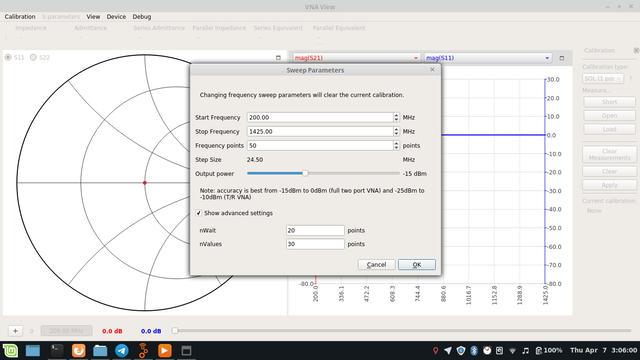
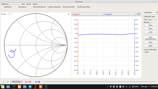
Consulting with NXP, the reference circuits are for when the transistor is biased to be Class-AB. Adequately modifying the load line impedance for class-A operation, and hence modifying the matching networks for these reference designs, I was able to get reasonably close. I also used simsmith to do a very crude form of load-pull (sweeping the complex output impedance of the transistor and observing what its equivalent 50-ohm transformed impedance looked like). Then, as a final step, I connected the NanoVNA along with attenuators and fine-tuned some trimmers to get a very nice match.
This approach worked rather well. *I even varied the drain current significantly to still see that the output matching was decent for different values, telling me that I've a good matching network.*
The problem appeared when I tried to tweak another of their reference design which combines two transistor stages
Here, these two are also presumably meant to run in class-AB, and I want them to run in class-A. One challenge here is that instead of matching between the stages (i/p of stage#2 and o/p of stage #1) is just a 1nF capacitor. There isn't a matching-to-50-ohm-and-back network as it would just make things inefficient.
I know I should much rather learn load-pull but for this iteration, the time to get a working amplifier is limited for me.
Anyway, I tweaked the output matching circuit, for what I "think" would work, but there were two problems. I'm dealing with a lot more gain here, and needed perhaps stronger attenuators. Also, the matching network, is perhaps poorly designed. When I'm at the Idq that I target - 4A, the match is good, but the match deteriorates much more significantly with different Idq values, than in the case of the original MRF300AN-reference design.
Anyway, it looks like for now, I will go with the two-independent-amp-stages for now, learn more about advance techniques for rf pa design (load pull and simulating in ADS) and reserve this effort for a future iteration.
I've tried to best capture the somewhat chaotic process I followed, but I do have two working amplifier stages giving be decent class-A performance which I was looking to consolidate the circuit of. If someone has more thoughts on how I could refine the design for a future setup, I will definitely keep in mind when coming back to this circuit.
73 // VU2TVE
